

Products


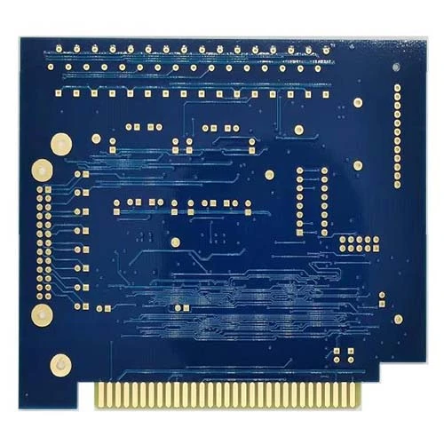
Sided Gold Finger Circuit Board
Viafull is one of leading China Sided Gold Finger Circuit Board manufacturer, supplier and exporters.
Send Inquiry
Product Description
Gold finger PCBs are those with gold finger-like pads, often used as edge connectors.
Chemical gold plating has excellent solderability, but the chemical deposition process means it is too soft and thin to withstand repeated wear. Gold plating is thicker and harder, making it ideal for re-plugging PCB edge connector contacts. Gold finger PCBs usually have to be chamfered at the edge connector to ensure easy insertion. Chamfering can be specified in the order details if specifically stated.
Gold fingers are the gold-plated posts you see on the connecting edge of a printed circuit board (PCB). The purpose of gold fingers is to connect auxiliary PCBs to the computer motherboard. PCB gold fingers are also used in a variety of other devices that communicate via digital signals, such as consumer smartphones and smart watches. Because the alloy has excellent electrical conductivity, it is used as a connection point on the PCB.
There are two types of gold suitable for PCB gold finger electroplating process:
Electroless nickel immersion gold (ENIG): This gold is more cost-effective and easier to solder than electroplated gold, but its soft, thin (usually 2-5u”) composition makes ENIG unsuitable for the wear and tear effects of circuit board plugging and unplugging. Electroplated hard gold: This gold is solid (hard) and thick (usually 30u”), so it is more suitable for the grinding effects of continuous use of PCBs.
Gold fingers enable different circuit boards to communicate with each other. From power to equipment, signals must pass between multiple contacts to execute a given command. When a command is pressed, the signal is passed between one or more boards before being read. For example, if you press a remote command on a mobile device, the signal is sent from the PCB-enabled device in your hand to a nearby or distant machine, which in turn receives the signal through its own circuit board. The process of plating gold fingers involves many meticulous steps. This ensures that every circuit board coming off the production line is equipped with the correct equipment to perfectly conduct the signal. The standards involved in the electroplating process also help ensure that the gold fingers on each circuit board perfectly match the corresponding sockets on a given motherboard. To ensure that all these gold fingers and sockets fit, each PCB All must pass a series of inspections and defect tests. If the gold plating on the circuit board is not smooth enough or does not adhere to the surface sufficiently, the results will not be good enough for commercial release. In order for the PCB gold finger to come together, the electroplating process must be carried out in a step where the details around the circuit board are first completed. When the fingers need to be plated, nickel is applied to the copper. Then, the surface finish is applied last. When everything is ready, the board is inspected under a magnifying glass and tested for adhesion.
During the PCB gold finger electroplating process, certain standards must be followed in order for the fingers to work properly. The design of the PCB itself must also consider the appropriate finger length and the area required for alignment.
Regardless of the purpose or size of the PCB itself, the following rules always apply to the design of the gold finger:
The plated through hole should not be close to the gold finger, the gold finger must not have any contact with the solder mask or silk screen, and the two should be kept at a certain distance, and the gold finger must always face the middle of the PCB (if you want an edge bevel) If any of these rules are not followed during the PCB gold finger electroplating process, the PCB may not be able to communicate with the mother board. Or, the PCB may not be properly inserted into the corresponding slot on the motherboard. Gold is used in Connector fingers on a PCB. The strength of gold allows gold fingers to be inserted and ejected hundreds of times without wearing out the connection contacts. Without the protection of gold plating, a circuit board could easily lose its connection after a few uses.
You may wonder why gold is better than other types of metals. After all, gold is one of the rarest and most expensive natural elements. Wouldn't it be more cost-effective to plate the connection edges of a PCB with copper or nickel? However, the required functionality of a printed circuit board requires gold. As PCBs evolved into their modern form, gold was determined to be the most suitable connection contact metal due to a number of factors. The main advantages of gold are the conductivity and corrosion resistance of the alloy. To increase strength, gold used in printed circuit boards is often combined with nickel or cobalt, which gives gold greater wear resistance in the face of constant PCB activity.
Data Sheet
| Product name: | Double-sided gold finger circuit board |
| Board: | FR4 |
| Number of layers: | 2L |
| Material: | S1141 |
| Board thickness: | 1. 6mm |
| Inner and outer layer copper thickness: | 1oz |
| Minimum aperture: | 0. 3mm |
| Surface treatment: | immersion gold |
| Line width: | 0. 15mm |
| Line spacing: | 0. 15mm |
| Others: | Electroplated gold finger |
Hot Tags: sided Gold Finger Circuit Board
Send Inquiry
Please feel free to fill your inquiry in the form below. We will reply you in 24 hours.


X
We use cookies to offer you a better browsing experience, analyze site traffic and personalize content. By using this site, you agree to our use of cookies.
Privacy Policy