

Products


8-layer PCB Circuit Board
Viafull is one of the professional 8-layer PCB Circuit Board manufacturer and supplier in China. Our products are CE certified and have in stock of factory, welcome to buy 8-layer PCB Circuit Board from us.
Send Inquiry
Product Description
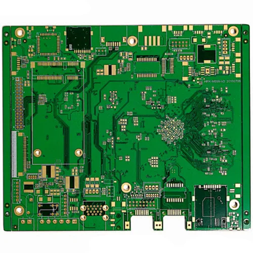
An 8-layer PCB Circuit Board is a multi-layer PCB that provides ample routing space for applications that require multiple power islands. This printed circuit board can help improve EMC performance by adding two planes.
This board is often mounted on compact devices such as motherboards, wearable watches, backplanes, etc. The increased cost of an 8-layer PCB justifies the added cost for excellent EMC performance. An 8-layer PCB stackup consists of 4 planes and 4 routing layers connected by 7 rows of dielectric material.
The PCB has a six-layer board for higher EMC performance. The 8-layer PCB is sealed with a solder mask on the bottom and top.
An 8-layer PCB stackup has many advantages that make it an ideal alternative to other circuit board materials. Here are the benefits of these PCBs;
Minimize fragility: An 8-layer PCB reduces the fragility of the device and improves overall performance. This helps protect the inner layers from noise, thereby reducing its vulnerability to external forces.
Reduce radiation: This type of multi-layer stackup helps eliminate any radiation that may occur in high-speed applications. Unlike other stackups, 8-layer PCB eliminates EMI radiation.
Lower operating costs: 8-layer PCB stackup is a cost-effective option. As for replacement and cleaning, this stack can save you a lot of money. This means that 8-layer PCB stackup requires little maintenance and is very durable.
Increased functionality: Choosing an 8-layer PCB will help increase the speed and functionality of the device used. Such a printed circuit board is more reliable and practical in different applications. This PCB has more than 4 layers of conductive materials to enhance signal routing.
8-layer PCB stackup applications
8-layer PCB stackup is the most common type of stackup in most electrical appliances. This multi-layer PCB can be used in a variety of applications such as:
Medical Industry
Automotive Industry
Manufacturing Industry
Chemical Processing Industry
Aerospace Industry
Hot Tags: 8-layer PCB Circuit Board
Send Inquiry
Please feel free to fill your inquiry in the form below. We will reply you in 24 hours.


X
We use cookies to offer you a better browsing experience, analyze site traffic and personalize content. By using this site, you agree to our use of cookies.
Privacy Policy