

Products


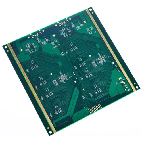
10-layer PCB Circuit Board
You can rest assured to buy 10-layer PCB Circuit Board from our factory and we will offer you the best after-sale service and timely delivery.
Send Inquiry
Product Description
10-layer PCB applications
Preamplifier, satellite antenna, GPS tracking device, SAN storage, AC drive, GSM signal booster, mobile broadband router, 220V inverter, memory module, car dashboard
10-layer manufacturing process
Cutting/baking materials—> Inner layer drilling—> Inner layer pattern transfer—> Inner layer line detection—> Etching/stripping—> Etching detection—> Browning—> Semi-cured sheet preparation—> Lamination—> Cutting copper foil—> Positioning—> Fitting—> Target hole—> Drilling—> Glue removal—> Copper immersion—> Graphic transfer—> Line detection—> Copper plating and tin plating—> Film removal and etching—> Tin removal—> Etching detection—> Dielectric detection test—> Solder mask detection—> Text—> Baking tray—> Spray tin, immersion gold, immersion tin—> Shape—> V cut—> Finished product test—> Anti-oxidation—> Final inspection—> Finished product extraction—> Packaging
Data Sheet
| Product name: | 10-layer PCB circuit board |
| Number of layers: | 10L |
| Sheet: | FR4 Tg170 |
| Board thickness: | 2. 4mm |
| Panel size: | 120*95mm/1 |
| Outer layer copper thickness: | 35μm |
| Inner layer copper thickness: | 35μm |
| Minimum through hole: | 0. 20mm |
| Minimum BGA: | 0. 25mm |
| Line width and line spacing: | 3/3. 2mil |
| Surface treatment: | immersion gold 2U'' |
Hot Tags: 10-layer PCB Circuit Board
Send Inquiry
Please feel free to fill your inquiry in the form below. We will reply you in 24 hours.


X
We use cookies to offer you a better browsing experience, analyze site traffic and personalize content. By using this site, you agree to our use of cookies.
Privacy Policy