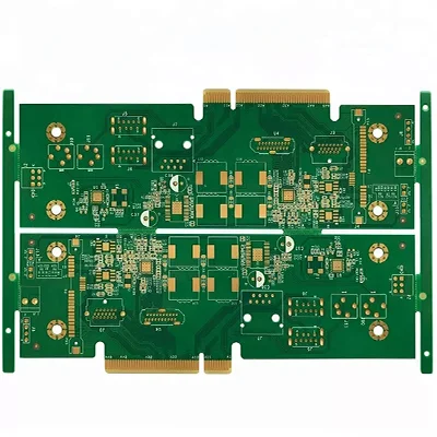
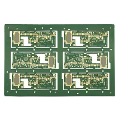
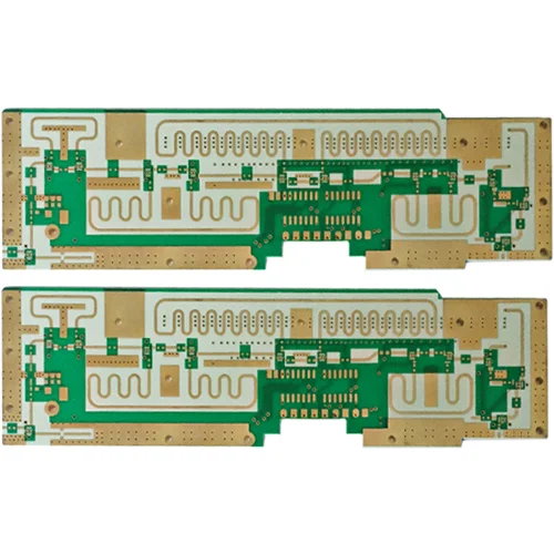
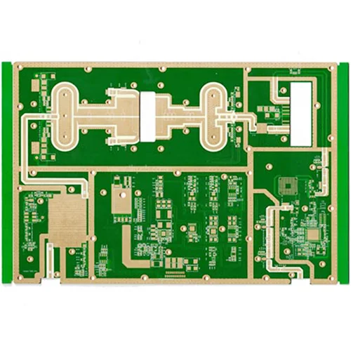
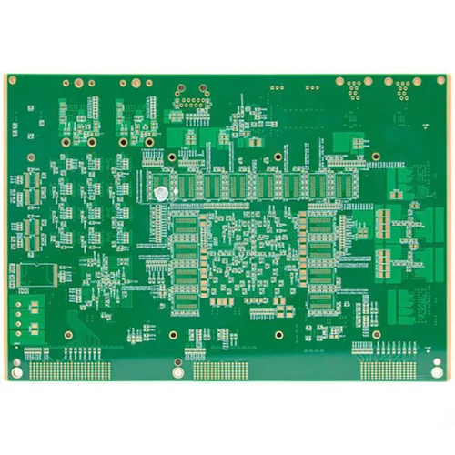
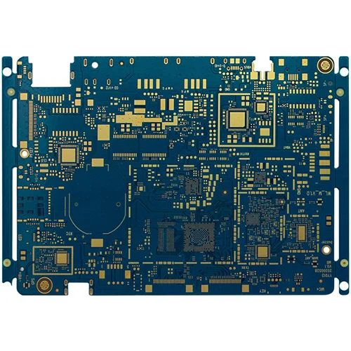
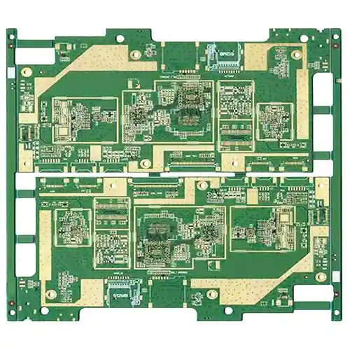
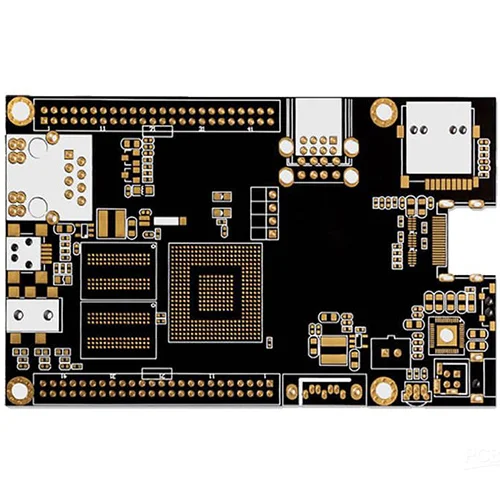
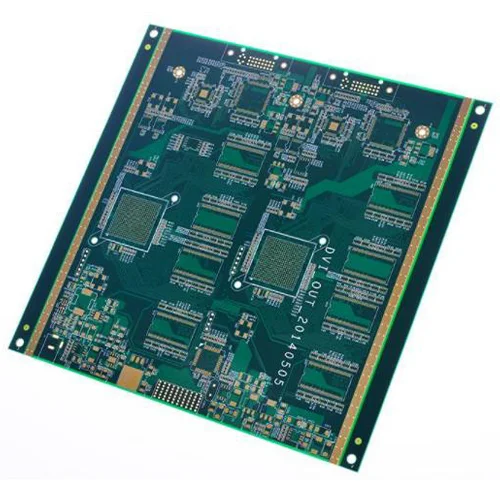
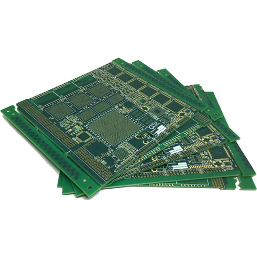
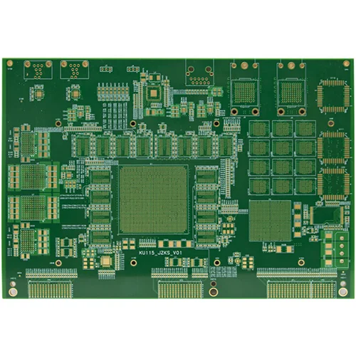
24-layer High-density High-speed PCB
Send Inquiry
What is a 24-layer PCB?
High quality 24-layer High-density High-speed PCB is offered by China manufacturer Viafull. Buy 24-layer High-density High-speed PCB which is of high quality directly with low price. A 24-layer PCB is an advanced multilayer board with 24 copper layers. The PCB includes a signal layer, a ground layer, and a power layer. Also, this PCB consists of silk screen, solder mask, etc. A 24-layer PCB is about 5mm thick. It provides dimensional stability due to the number of layers in it.
The manufacturer arranges the ground layer and the signal layer effectively. This helps ensure that the PCB is compatible with HDI applications. These applications are high-density interconnects. The materials used in the 24-layer PCB ensure a low dielectric constant. Also, the dielectric material used in this advanced multilayer board is thin. So this helps create tight coupling between the layers.
Materials of 24-layer PCB
A 24-layer PCB contains different materials in its manufacturing process. It uses materials such as copper foil, FR4, CEM3, and epoxy resin. In this PCB, the manufacturer laminates the copper foil and glass fiber resin material together. FR4 is a PCB material that provides enough rigidity in electronics. It provides enough glass transition temperature.
Furthermore, the material has excellent moisture resistance. This means that PCBs containing FR4 can withstand high temperatures. Moreover, this material has suitable dielectric strength.
Silkscreen, FR4, and solder mask are the base materials of 24 layer PCBs. High glass transition temperature is an important feature of 24 layer PCBs.
Other materials used in 24 layer PCB manufacturing include copper foil and prepreg. 24 layer PCBs can have different copper thicknesses. The thickness of copper and the number of layers help it conduct high current loads.
What is 24 layer PCB stackup?
24 layer PCB stackup is the arrangement of upper layers on the circuit board. In a multi-layer PCB, there are several ways to place copper layers on the board. Manufacturers consider several important factors before arranging a multi-layer stackup.
In a 24 layer stackup, there are routing layers, ground layers, and power layers. Routing layers can be top, middle, or bottom layers. Ground and power layers are very important in this stackup.
Routing layers create interconnections between components. Manufacturers can place the wiring layer on the bottom, top, or middle layers. This depends on the application requirements of the board. Signal routing is a critical part of a multilayer board. The stackup structure of a 24-layer PCB determines its functionality. A well-aligned stackup will ensure signal routing in the PCB.
24-Layer PCB Manufacturing
The manufacturing of a 24-layer PCB involves certain processes. Since this PCB has ten layers of conductive material, its manufacturing is complex. Manufacturers laminate the core and prepreg layers under high pressure and high temperature.
During this process, manufacturers ensure that there is no air between the PCB layers. They also ensure that the adhesive that secures the layers melts properly. A 24-layer PCB consists of a variety of materials. The core and prepreg are similar materials. However, the prepreg is more ductile than the core. This is because it is not fully cured. When manufacturers apply high temperatures to the stackup, the prepreg melts. The layers are then connected together. After cooling, the result is a solid 24-layer board. Manufacturers apply solder mask to the multilayer board. The role of the solder mask is to prevent the traces from shorting. The inner layers of a multilayer board include fiberglass and epoxy core, and prepreg laminates these layers together. Manufacturers stack the inner layers together to ensure that the layers are aligned.
The production process of a 24-layer PCB is briefly described as follows:
Inner layer imaging and etching
Inner layer lamination
Drilling board
Outer layer imaging
Plating and etching
Outer layer etching stripping
Solder mask
Screen printing
Testing
Advantages of 24-layer PCB
This PCB helps to enhance the functionality of electronic devices. The 24-layer board has great advantages that are required for the project. Some of these advantages are:
Compact design
The 24-layer PCB supports compact design. The ground layer and signal layer of the PCB overlap each other. This board is ideal for small devices such as laptops, mobile phones, etc. Electronic devices are getting smaller and more complex. The 24-layer PCB is ideal for complex and miniature devices.
Suitable for different temperatures
The 24-layer PCB can work at different temperatures. This PCB is designed to work at different temperatures. The 24-layer board is ideal for high-performance and high-end applications.
High Current Conduction
Another important advantage of this type of PCB is the ability to carry high current loads. The PCB is available with different copper thicknesses. It can withstand high power.
High Functionality
24-layer PCBs are very practical. Therefore, they are widely used in high-density interconnection and high-power projects. In addition, PCBs also improve the efficiency of high-speed projects.
Data Sheet
| Name: | 24-layer high-density high-speed PCB |
| Material: | TU872SLK |
| Number of layers: | 24 |
| Thickness: | 3. 2±0. 32mm |
| Minimum diameter of mechanical hole: | 0. 25mm |
| Minimum track/pitch: | 75/75um |
| Minimum board thickness to aperture ratio: | 12. 8:1 |
| Surface treatment: | ENIG 0. 05um |
| Application areas: | Aerospace |


