Products
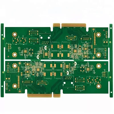
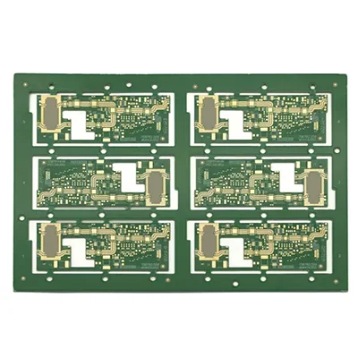
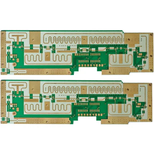
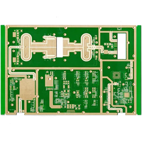
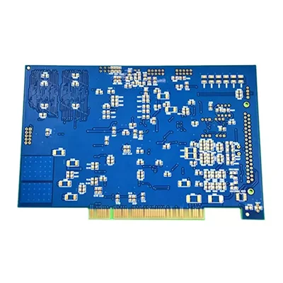
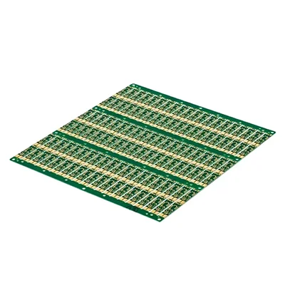
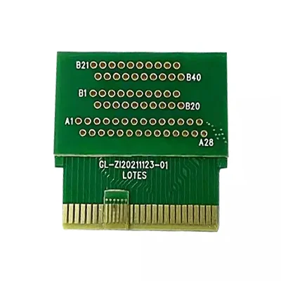
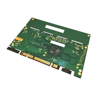
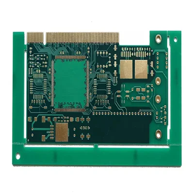
Multi-layer Gold Finger Motherboard Control PCB
For you, we can offer better pricing and competent service. Should you be intrigued by Multi-layer Gold Finger Motherboard Control PCB, kindly get in touch with us. We adhere to the standard of conscience-driven, committed service at the cost of quality assurance.OneWe adhere to the standard of conscience-priced, devoted service, so you can feel secure.
Send Inquiry
Product Description
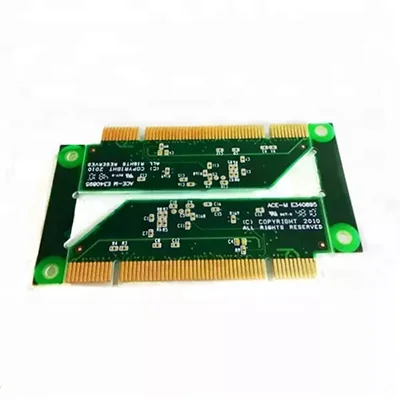
Detailed processing of PCB gold fingers:
1. For PCB boards that need to be frequently plugged and unplugged, the gold fingers generally need to be hard-plated to increase the wear resistance of the gold fingers.
2. The gold fingers need to be tilted backwards, generally 45°, other angles such as 20°, 30°, etc. If the design does not tilt backwards, there is a problem. The arrow in the figure below shows a 45° tilt angle:
3. The gold finger needs to make a whole welding window. The PIN does not need to open the steel mesh;
4. The minimum distance between Shenxi and Shenyin pads is 14 million. It is recommended that the pad be more than 1mm away from the finger position, including the via pad;
5. Do not apply copper on the surface of the gold finger.
Data Sheet
| Name: | Multi-layer gold finger motherboard control PCB |
| Type: | Multi-layer circuit board |
| Number of layers: | 6 layers |
| Base material: | FR4, aluminum, high Tg FR4 |
| Copper thickness: | 0. 5-1 ounce |
| Board thickness: | 0. 4-4. 0mm |
| Aperture: | 0. 15-0. 2mm |
| Line width: | 0. 1-0. 3mm |
| Line spacing: | 0. 1-0. 3mm |
| Surface treatment: | immersion gold, tin spraying, gold finger |
| Solder mask: | green |
Hot Tags: Multi-layer Gold Finger Motherboard Control PCB
Send Inquiry
Please feel free to fill your inquiry in the form below. We will reply you in 24 hours.
X
We use cookies to offer you a better browsing experience, analyze site traffic and personalize content. By using this site, you agree to our use of cookies.
Privacy Policy


